Researchers have directly imaged the electrostatic landscape inside a single moiré unit cell for the first time, using a new atomic-scale sensor built from a single defect in a two-dimensional material.
 Study: Imaging the sub-moiré potential using an atomic single electron transistor. Image Credit: MZinchenko/Shutterstock.com
Published in Nature, the study introduces an atomic single electron transistor (SET) that achieves ~1 nm spatial resolution and a potential sensitivity of 5 μV Hz-1/2.
Built on the quantum twisting microscope (QTM) platform, which enables the formation of pristine, scannable interfaces between van der Waals (vdW) materials, the probe can resolve the sub-moiré potential landscape in graphene aligned to hexagonal boron nitride (G/hBN).
This canonical moiré system’s electrostatic structure has previously only been inferred indirectly.
Get all the details: Grab your PDF here!
Electrons in solids move through periodic potential landscapes set by atomic structure. In conventional materials, those potentials vary on atomic length scales, making them nearly impossible to image directly.
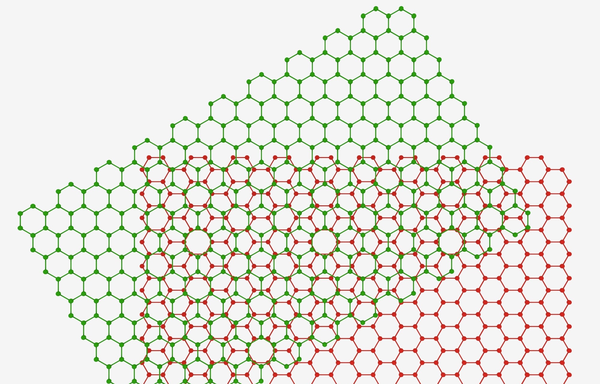
Moiré engineering changes that. When two slightly mismatched lattices are stacked together, like graphene and hexagonal boron nitride, they form a larger-scale periodic pattern.
In aligned G/hBN, this produces a moiré superlattice with a wavelength of approximately 14 nm, dramatically larger than atomic spacing and key to many unexpected quantum phenomena.
Despite its importance – including roles in Hofstadter physics, correlated states, and fractional quantum anomalous Hall phases – the G/hBN moiré potential itself had never been directly mapped.
Scanning single-electron transistors are among the most sensitive tools available for measuring electrostatic potentials, but their lithographic dimensions (>100 nm) limit their spatial resolution, preventing them from resolving structure within a moiré unit cell.
Other scanning probes have achieved high resolution in molecular systems, but not in buried vdW heterostructures.
Using an Atomic Defect as a Quantum Sensor
The new approach replaces a lithographically defined island with a single atomic defect embedded in a thin transition metal dichalcogenide (TMD) layer. That defect is essentially a quantum dot.
In the experiment’s inverted geometry, the system of interest, aligned G/hBN, is mounted on the QTM tip and scanned over the stationary defect.
As the spatially varying electrostatic potential (r) passes over the defect, it shifts the defect’s Coulomb blockade peak. Tracking that shift directly maps the local potential.
The device achieves approximately 1 nm spatial resolution, which makes it two orders of magnitude finer than conventional scanning SETs, with a potential sensitivity of 5 μV Hz-1/2.
This sensitivity and resolution correspond to detecting variations of just a few parts per million of the potential generated by a single electron charge at that distance.
By adding top and bottom gates, the researchers use the defect as a spectroscopic probe.
The curvature of the resulting Coulomb diamonds reflects the electronic compressibility of the graphene layers, allowing local thermodynamic properties to be measured alongside the electrostatic potential.
A Strong and Symmetric Potential
The resulting maps reveal a clear triangular moiré lattice with a wavelength of ~14 nm.
More strikingly, the electrostatic potential inside each unit cell shows an approximate C6 symmetry – nearly sixfold rotational symmetry – rather than the C3 symmetry typically expected for unrelaxed G/hBN structures.
The potential amplitude is substantial: approximately 60 mV peak-to-peak, ranging from 52 to 62 mV depending on filling. Even at zero carrier density (ν ≈ 0), the amplitude remains large.
Across fillings where ν = 1 corresponds to one electron per moiré unit cell, the amplitude changes by only about 10 %, indicating that the moiré potential is largely set by intrinsic interface properties, rather than carrier screening.
Theory Matches Symmetry, Not Magnitude
To interpret the measurements, the researchers model three contributions to the moiré Hamiltonian: a stacking pseudopotential, a deformation pseudopotential arising from lattice relaxation, and a pseudomagnetic field term.
Individually, the leading stacking and deformation terms each exhibit strong C3 symmetry. However, their contributions partially cancel, producing a combined potential with near-C6 symmetry – consistent with experiments.
Self-consistent Hartree calculations show that electronic screening reduces the magnitude of the pseudoelectric potentials by roughly a factor of two while preserving their spatial structure.
The pseudomagnetic and mass-term contributions are small, scale linearly with filling, and vanish at ν = 0, consistent with the weak carrier-density dependence observed experimentally.
Yet the theoretical total potential is only about half as large as the measured ~60 mV.
The authors consider whether underestimated strain could explain the discrepancy, but increasing strain alone would enhance C3 symmetry rather than produce the near-C6 symmetry observed.
This gap between theory and experiment points to an incomplete understanding of this extensively studied interface.
Why is Atomic-Scale Proximity Important?
The team also measured how the potential decays with distance from the interface.
Two defects located approximately 0.8 nm and 1.5 nm from the G/hBN interface showed about a 60 % reduction in amplitude between those heights.
The decay is steep. Extrapolation suggests that at distances comparable to the moiré wavelength, the detectable signal would drop to a negligible fraction of its interface value.
The result highlights the importance of atomic-scale proximity and why earlier probes positioned farther away could not capture the full potential landscape.
A Future of Atomic-Scale Resolution?
The atomic SET combines nanometre-scale spatial resolution with exceptional potential sensitivity inside pristine vdW interfaces.
Beyond G/hBN, the technique forges a path to imaging charge order and thermodynamic structure in a huge range of quantum systems, including Wigner crystals, topological edge states, vortex charges, symmetry-broken phases, and fractionally charged quasiparticles.
As moiré materials continue to serve as platforms for correlated and topological states, direct potential imaging could become a key tool for testing theory and guiding device design in next-gen 2D heterostructures.
Journal Reference
Klein D.R. et al. (2026). Imaging the sub-moiré potential using an atomic single electron transistor. Nature. DOI: 10.1038/s41586-025-10085

